Table Of Content
The schematic is a visual representation of the circuit that shows how the components are connected and how they interact with each other. It serves as a blueprint for the PCB layout and is important for ensuring that the final board functions as intended. The schematic consists of various symbols that represent different electronic components such as resistors, capacitors, transistors, and integrated circuits. These symbols are interconnected by lines that indicate the electrical connections between the components.
Ceramics Used in Electronic Applications
A typical PCB consists of multiple layers, each serving a specific purpose in the overall design. The conductive layers, usually made of copper, are used for routing electrical signals and power between components. The number and arrangement of these layers depend on the complexity of the design and the required functionality. Many of the important performance characteristics of a PCB are defined in the stack-up or the arrangement of layers in the PCB. The layer stack-up is built with alternating layers of conductive and insulating material, and with alternating layers of core and prepreg (two types of dielectrics used in the layer stack-up).
Power It Up, Power it Down
Later, the metal strips were replaced by wires connected to screw terminals, and wooden bases were replaced by metal frames. This let things be smaller, which was needed as circuits became more complex with more parts. In 1925, Charles Ducas of the United States developed a method using electroplating.
To Design For High Speed Data Rates
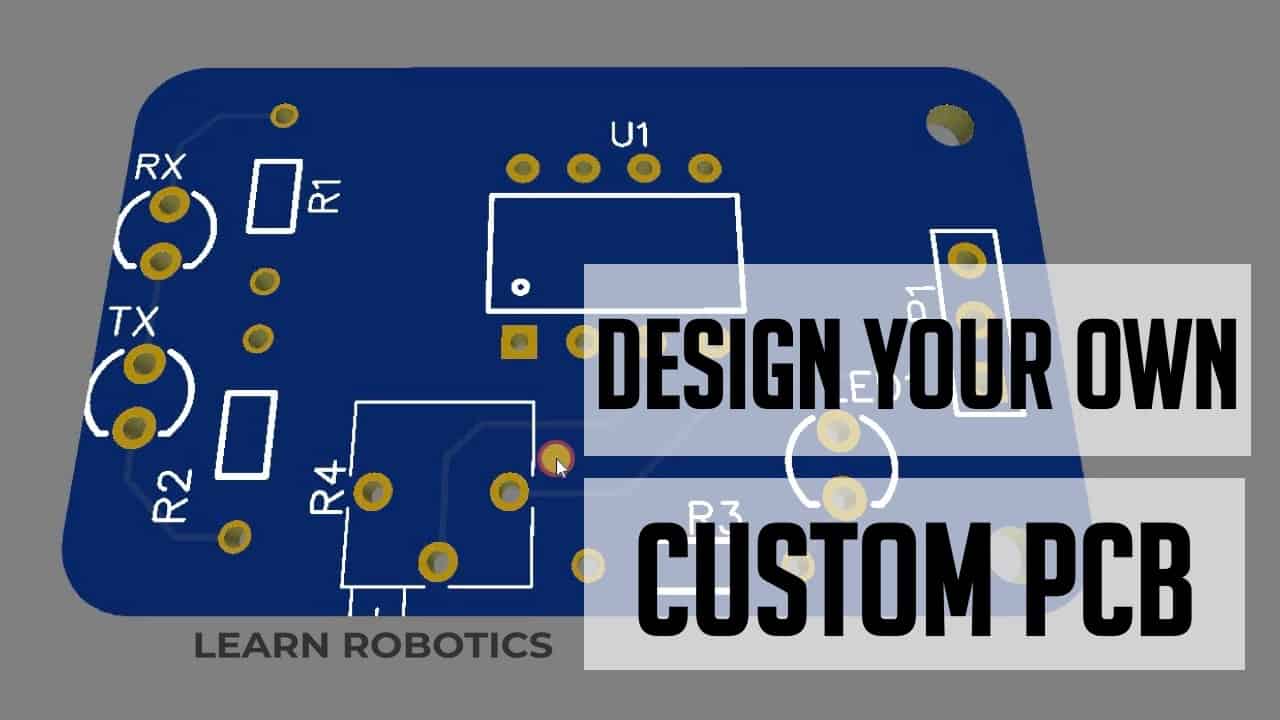
With these parts ready for use, begin by organizing them on schematic sheets within the CAD tools. Once the parts are roughly placed, wires can be drawn that represents the connectivity between the pins of the schematic symbols. These lines are known as nets, and they can represent single nets or groups of nets for memory or data circuits. During the schematic capture, process parts must be moved as needed to create a schematic that is legible and clear. This manufacturer uses electronic design automation tools to solve complex issues. Soon, the Internet of Things and the 5G market will create more opportunities for this industry.
Verify the changes (addition of the SchDoc information to the project without error) by clicking on the Validate Changes tab. If the status for all items is green, then click on the Execute Changes tab. Altium Designer can save you a substantial amount of time during this PCB design step. The white silkscreen layer is applied on top of the soldermask layer.
PCB Board Design: The Ultimate Guide to Great Printed Circuit Board Layout
Renesas to acquire Altium for $5.91 billion - ENGINEERING.com
Renesas to acquire Altium for $5.91 billion.
Posted: Thu, 15 Feb 2024 08:00:00 GMT [source]
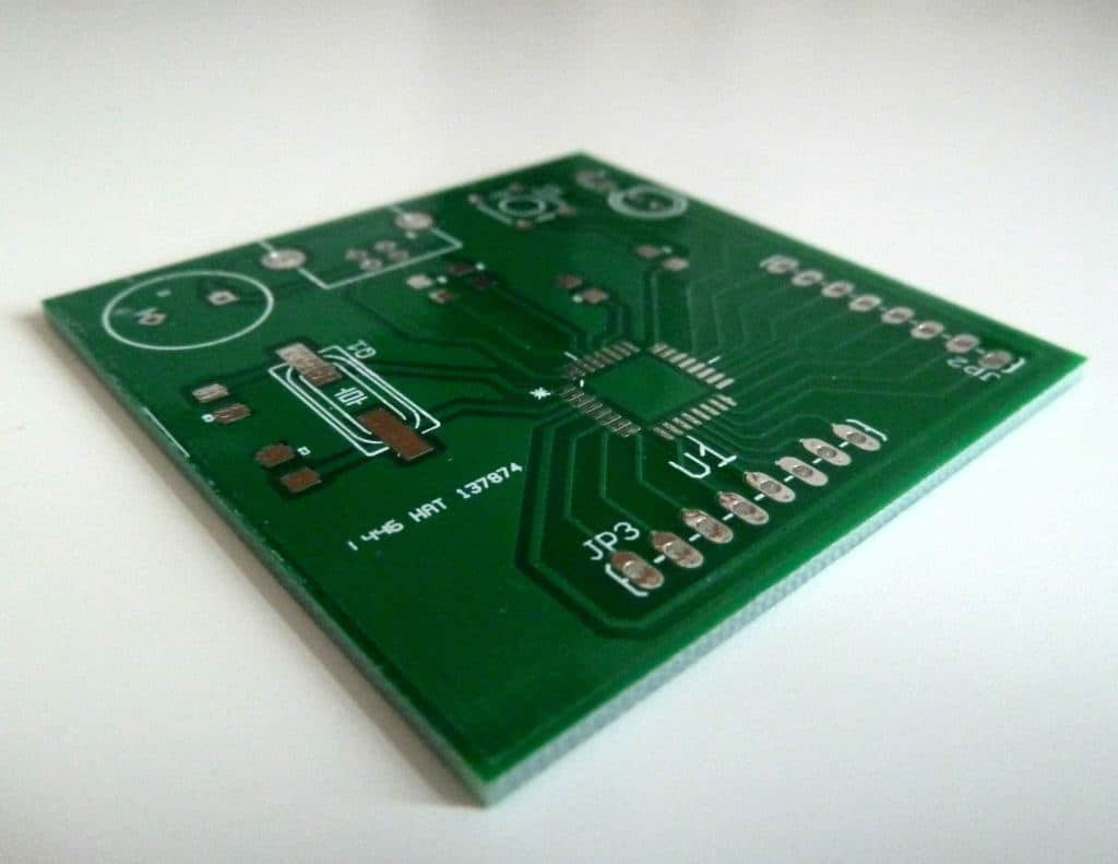
This process includes etching all of the traces and planes onto the different metal layers and compressing them together, producing a bare board that is ready for assembly. Flexible boards are composed of a less rigid material that allows for far greater deflection. The material is tactilely reminiscent of a film roll, and the board thickness is usually far less than a standard rigid board. While they already see major usage, there is hope that flexible boards will usher in the next step of wearable technology and remove the current planar constraints inherent to rigid board devices. PCBs — which house and interconnect chips, transistors and other components — typically consist of layers of thin glass fiber sheets coated in hard plastic and laminated together with copper.
Working with Power Supply Design Tools
The advanced PCB technologies offer unique features and capabilities, enabling the development of more compact, flexible, and high-performance electronic devices. Looking ahead, PCB technology is expected to continue advancing to meet the ever-increasing demands for miniaturization, high-speed performance, and enhanced functionality in electronic devices. Vias are the small holes drilled through the PCB and plated with conductive material, allowing for electrical connections between different board layers.
This information is valuable for troubleshooting and fine-tuning the circuit design. Printed Circuit Boards (PCBs) are essential components in modern electronic devices. They provide a platform for connecting and supporting various electronic components, allowing them to function together seamlessly. Creating your own PCB may seem like a difficult task, but with the right tools and knowledge, it can be a rewarding and cost-effective endeavor.
PCBs Past and Present
The unified design rules-driven environment in Altium Designer lets PCB designers easily create schematic drawings, a PCB layout, and manufacturing documentation in a single environment. After configuring your printed circuit board workspace, layers, grids, and design rules, your design team can arrange components and route traces throughout a circuit board layout. The PCB Editor supports the 32 signal layers, 16 internal power plane and ground plane layers, and 32 general purpose mechanical, special, and non-electrical layers. Altium Designer displays attributes for all layers in a color-coded workspace.
Components are soldered to the board onto metal pads, which are connected to the board circuitry. A board can be composed of one, two, or multiple layers of circuitry. Single-sided PCBs are the simplest type of printed circuit board, consisting of a non-conductive substrate, typically made of FR-4 material, with conductive traces and components on only one side.
Conventionally, semi-cured PCB layers are held in cool, dry conditions where they have a limited shelf life before they're laminated in a heat press. Because trimers can form new bonds, researchers laminated fully cured PCB layers. PCBs—which house and interconnect chips, transistors, and other components—typically consist of layers of thin glass fiber sheets coated in hard plastic and laminated together with copper. That plastic can't easily be separated from the glass, so PCBs often pile up in landfills, where their chemicals can seep into the environment. The team tested its vPCB for strength and electrical properties, and found that it performed comparable to the most common PCB material (FR-4).
Rigid-flex PCBs offer the best of both worlds by combining rigid and flexible substrates into a single board. The rigid sections provide structural support and accommodate components that require stability, while the flexible sections allow for bending and folding in specific areas. This unique combination enables the creation of three-dimensional designs and the integration of multiple circuit boards into a single assembly. Rigid-flex PCBs find applications in space-constrained devices like smartphones, laptops, and medical implants, where reliability and compact packaging are essential.


No comments:
Post a Comment